博士課程学生募集
他大学からの入学,社会人ドクターを歓迎します。これまで2名が博士号を取得しています。2名とも在籍期間3年で学位を取得しました。1名は大学の教員として活躍しています。もう1名は現在,海外企業(海外在中)で働いています。少しでも興味があれば,北村 (kitamura[at]eedept.kobe-u.ac.jp) までご連絡ください。例年8月の入試でその年の10月,2月の入試で4月の入学が可能です。
[募集要項]
入試情報
お知らせ
2026年4月1日 4年生10人が配属になりました。[Link]2025年4月1日 4年生11人が配属になりました。[Link]
2025年2月1日 張 益仁助教がメンバーに加わりました。[Link]
2024年4月1日 4年生9人が配属になりました。[Link]
2024年3月24日 応用物理学会で服部准教授が研究発表を行いました。[Link]
2023年11月10日 薄膜材料デバイス研究会で4件の研究発表を行いました。[Link]
2023年11月1日 服部准教授による透明極薄膜(0.3nm)の光学顕微鏡による可視化に関する研究が学術雑誌 ACS Applied Nano Materials に掲載されました。[Link]
2023年10月24日 北村教授による有機トランジスタの標準材料であるpentaceneに関するレビュー論文のgoogle scholarでの被引用回数が300回を超えました。[abstract]
2023年10月2日 InGaZnO上への単分子膜形成に関する研究内容が学術雑誌に掲載されました。[abstract]
2023年5月18日 河合塾 みらいぶっく 「デバイス関連化学」の注目の研究者で取り上げられています。[ウェブ]
2023年2月22日 第70回応用物理学会 [春季学術講演会] (3/15-3/18) で以下の発表を行いました。
[15p-PA03-10]
有機薄膜形成のためのインクジェット法による親水疎水パターニングを用いた液摘挙動制御
[15p-E102-7]
スパッタリングにより作製したIn5GaZnO10薄膜トランジスタの特性評価
[15a-PA01-44]
層状物質の厚い膜に存在する単層分の厚さの違いを検知する手法
2023年1月26日 北村教授のキャリアセンター長としてのインタビュー記事が日経産業新聞に掲載されました。[ウェブ]
2023年1月23日 森 敦紀 先生との共同研究による成果が学術雑誌に掲載されました。[abstract]
2022年12月7日 服部助教 の研究成果が学術雑誌に掲載されました。[abstract]
2022年10月1日 北村教授が留学生就職促進シンポジウム(@東京大学)で本学の「留学生就職促進プログラム」の現状について講演を行いました。[ウェブ]
2022年9月29日 北村教授が2022年度膜工学秋季講演会・膜工学サロンで「薄膜材料デバイスのための界面制御」と題して講演を行いました。[ウェブ]
2022年8月29日 ウエブページのデザインを新しくしました。
はじめに
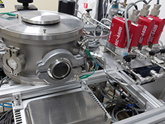
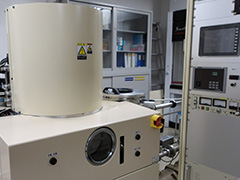
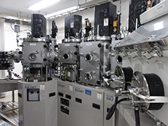
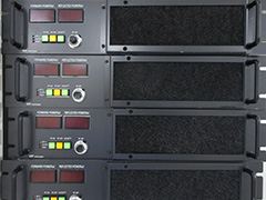
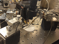
ここは,神戸大学大学院工学研究科電気電子工学専攻量子機能工学(EP3)北村・服部・張研究室のウェブページです。 当研究室では,薄膜材料を使った電子デバイスの開発とそれに関係する基礎研究を行っています。ここでいう薄膜とは,数10~数100 nm の厚さの膜を言います。 薄膜を使った応用としては電界効果トランジスタ,ガスセンサ,LED,太陽電池が考えられますが,当研究室が得意とするのは電界効果トランジスタです。 これまで,有機半導体や酸化物半導体の薄膜を使った電界効果トランジスタに関する研究での実績があります。 薄膜としては,半導体,金属,絶縁膜がありますが,当研究室ではこれらを製膜するための各種装置を有しています。 無機材料については,主にマグネトロンスパッタを使用しています。有機半導体については,専用の蒸着装置を所有しており,高品質の膜を製膜することができます。また,溶液プロセスとして,インクジェット法のほか,スピンコート法,ブレード法での製膜も可能です。 デバイス開発に関係して,薄膜の表面処理や表面への単分子膜の形成に関する技術を有しています。This is the web page of Kitamura-Hattori-Chang Laboratory, Department of Electrical and Electronic Engineering, Graduate School of Engineering, Kobe University. Our laboratory develops electronic devices using thin film materials and conducts basic research related to them. A thin film here means a film with a thickness of several tens to several hundred nm. Applications using thin films include field effect transistors, gas sensors, LEDs, and solar cells. We mainly focus on field effect transistors. we have developed high-performance field effect transistors using thin films of organic semiconductors and oxide semiconductors. Thin films include semiconductors, metals, and insulating films, and our laboratory has various equipment for forming these films. For inorganic materials, we mainly use magnetron sputtering. For organic semiconductors, we deposit the films using vapor deposition systme that produces high-quality films. As a solution process, we can deposit organic films by inkjet method, spin coating method, and the blade coating method. In relation to device development, we have technology related to surface treatment of thin films and the formation of monomolecular films on surfaces. In relation to device development, we have technique related to surface treatment of thin films and the formation of molecular layers on the surfaces.